Etched - Transformer-Specific AI Chip Sohu
Etched has developed a specialized ASIC for Transformer models, offering 8x performance over NVIDIA Blackwell. The A0 chip delivers 10x efficiency.
Introduction
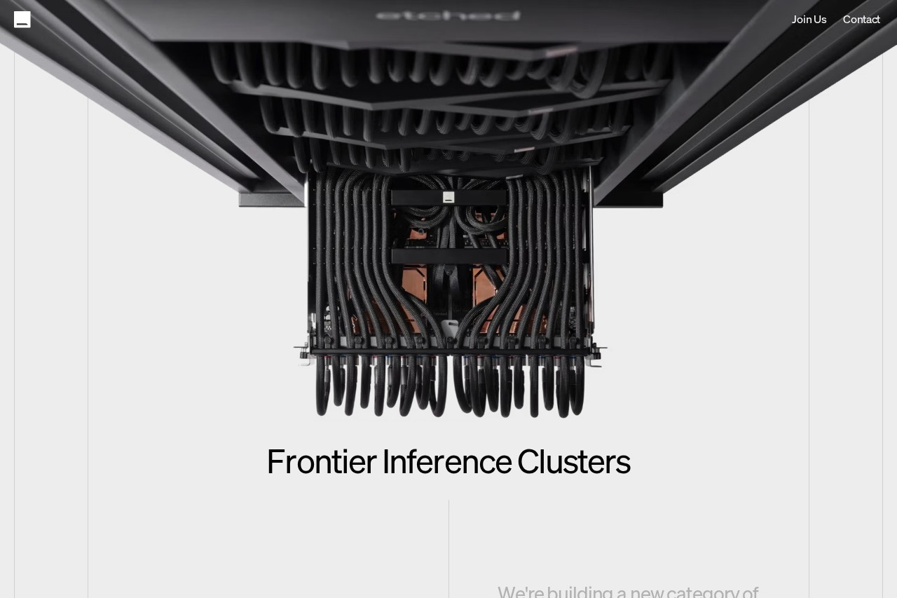
Etched is an AI chip startup headquartered in Cupertino, California, founded in 2022 by Harvard dropouts Gavin Uberti and Chris Zhu. The company focuses on building Frontier Inference Clusters, with its core product being Sohu, an ASIC chip purpose-built for the Transformer architecture. Etched claims Sohu is an order of magnitude faster than NVIDIA's upcoming Blackwell GPU while also being more cost-effective. The team at Etched numbers over 400 people, with talent drawn from top semiconductor companies including NVIDIA, Google TPU, Broadcom, SK Hynix, and TSMC. The company has raised a total of $800 million across four undisclosed funding rounds plus strategic investments, reaching a valuation of $5 billion. Its A0 chip has already come back from TSMC's N4P process node, and the first rack-scale products have secured over $1 billion in customer contracts, with shipments expected this summer.
Key Features
- Sohu Chip: A dedicated ASIC purpose-built for Transformer models, delivering inference speeds more than 20x faster than NVIDIA's existing H100 systems on AI models currently in training.
- Low-Voltage Inference (LVI): A proprietary architecture that runs compute modules at less than half the voltage of traditional AI chips, achieving multiple times the FLOPS density and sustaining 80%+ peak FLOPS on trillion-parameter sparse MoE models without thermal throttling.
- Cluster-Scale Memory (CSM): A hybrid HBM/SRAM design that creates a shared memory pool across chips via a proprietary ultra-low-latency, high-bandwidth interconnect, balancing high throughput with low latency.
- Full-Stack Co-Design: From transistor to token, the chip, package, PCB, cold plates, and interconnect are all co-optimized to support trillion-parameter MoE models, long-context workloads, and agent-based applications.
Highlights
- Delivers 8x the performance of NVIDIA Blackwell on Transformer inference, with a single 8-chip Sohu server processing over 500,000 Llama 70B tokens per second.
- Backed by a 400+ person engineering team recruited from NVIDIA, Google TPU, Broadcom, SK Hynix, and TSMC, led by Harvard-dropout founders.
- A0 chip has been taped out on TSMC's N4P process and validated, with over $1 billion in customer orders already secured.
- Follows the proven playbook of Google TPU: going all-in on a specialized architecture for a single dominant workload rather than trying to be a general-purpose solution.
- Operational infrastructure spans a factory in Taiwan and a data center, test center, and NPI prototyping lab in San Jose, targeting gigawatt-scale deployment.
Who It's For
Etched is built for organizations running large-scale Transformer inference workloads, including cloud service providers looking to lower total cost of ownership by replacing portions of their GPU clusters, and AI teams serving models like Llama or GPT that need maximum throughput at minimum cost. It is also well suited for long-context and agent-based applications that demand high throughput while maintaining low interactive latency, making it a compelling option for any operation where Transformer inference performance and cost efficiency are the top priorities.